Deep Research & Description
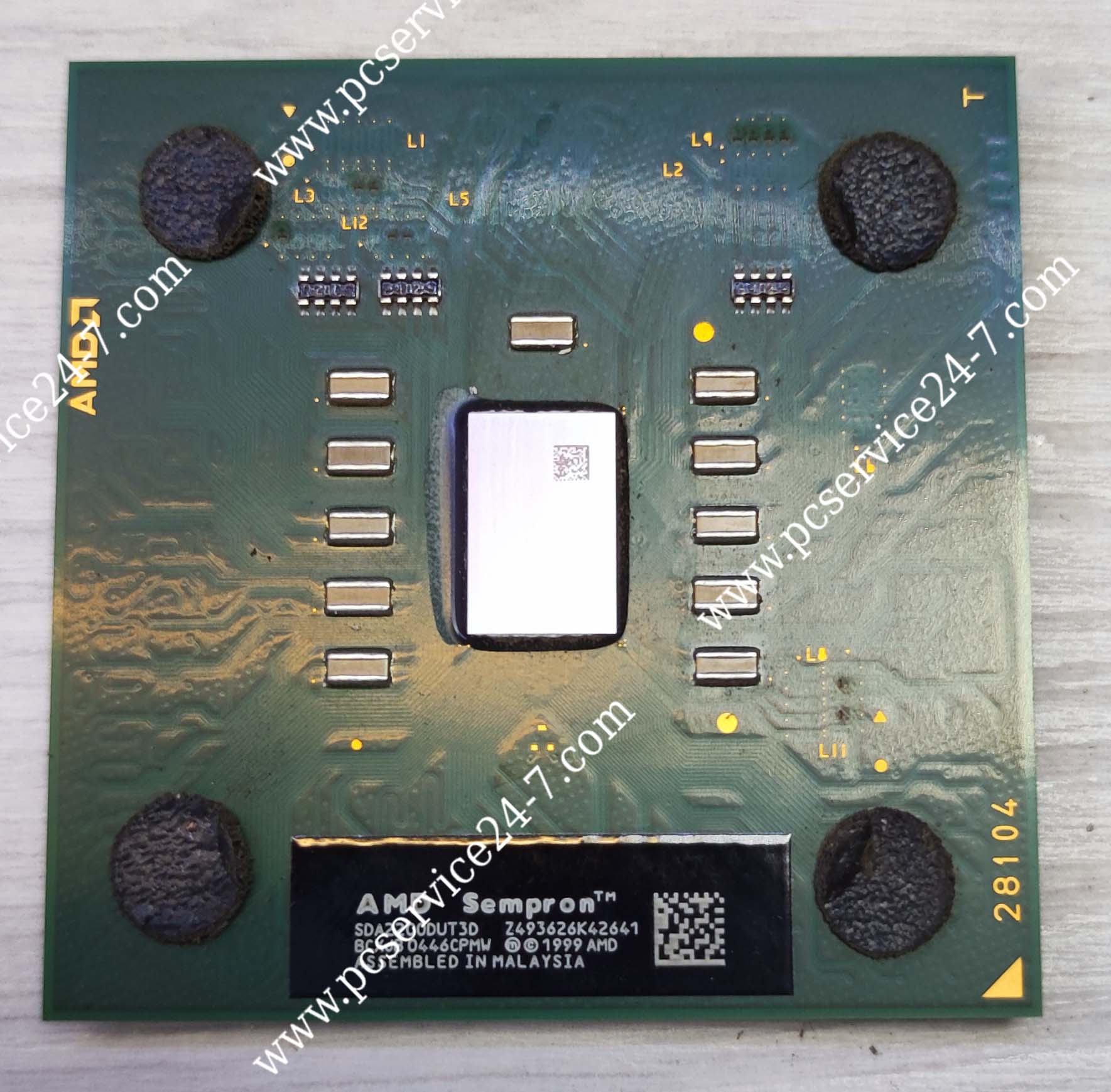
The “2200+” model running at 1500 MHz is technically based on the Thoroughbred-B or Thorton core. Its most significant feature is the jump to the 333 MHz Front Side Bus (FSB). While earlier “Value” chips were often stuck on the aging 266 MHz bus, this chip utilized the faster 166 MHz (DDR 333) path, allowing it to communicate with the newer PC2700 DDR RAM at full speed. This solved a major data bottleneck for budget systems of the time.
Architecturally, this was a 32-bit warrior. Even though AMD had already launched the 64-bit era with Socket 754 and 939, the Sempron 2200+ was kept alive to provide a low-cost, low-heat option for office and home PCs. It utilized the 9.0x multiplier ($166.6 \text{ MHz} \times 9 = 1500 \text{ MHz}$). Because it was based on the mature 130nm process, it was famously cool-running and became a favorite for “silent PC” enthusiasts who wanted decent performance without the screaming fans of the Pentium 4 era.
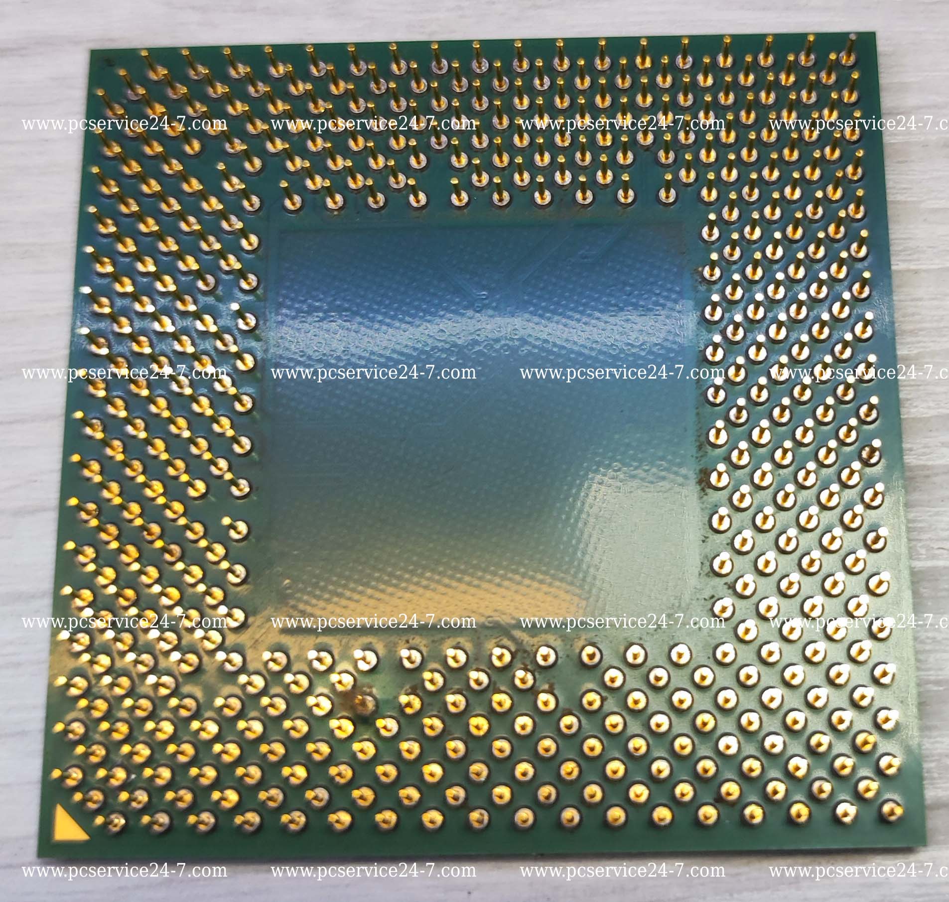
In the evolution of the PC, the Sempron 2200+ was the “last stand” of the Socket A (Socket 462). It allowed users with older motherboards to perform one final, cheap upgrade that could still handle the modern web and basic multimedia tasks of the mid-2000s. It was the chip that proved the Athlon XP’s architecture was so efficient it could still compete in the budget market years after its initial debut.
Era Context
-
The Rebranding: This chip was essentially an Athlon XP “under the hood,” but rebranded as Sempron to distinguish it from AMD’s new 64-bit processors.
-
Operating System: The perfect match for Windows XP Service Pack 2.
-
Legacy: Many of these chips are still found today in industrial machines and old arcade cabinets because of their incredible reliability and low heat output.
-
Overclocking: Because it ran on the 333 MHz bus with a low 9x multiplier, many users found they could easily push the bus to 400 MHz (DDR400), instantly turning this 1.5 GHz chip into an 1.8 GHz powerhouse.
Component Gallery
Quick Specs
| Feature | Specification |
| Model | Sempron 2200+ |
| Actual Clock | 1500 MHz (1.5 GHz) |
| Bus Speed | 333 MHz (FSB) |
| L2 Cache | 256 KB (Full Speed) |
| Core Codename | Thoroughbred-B / Thorton |
| Socket | Socket A (Socket 462) |
| Architecture | 32-bit (x86) |
| Manufacturing Process | 130 nm (0.13 micron) |
| TDP (Power) | 62 Watts |
| Voltage | 1.6 V |